
Look, PCB layout isn’t exactly casual conversation material. But whether you’re an engineer, designer, or startup founder, getting it right is critical. Messy layouts can derail your entire project.
So let’s untangle this web of traces, vias, and layers—clear, practical, and easy to follow.
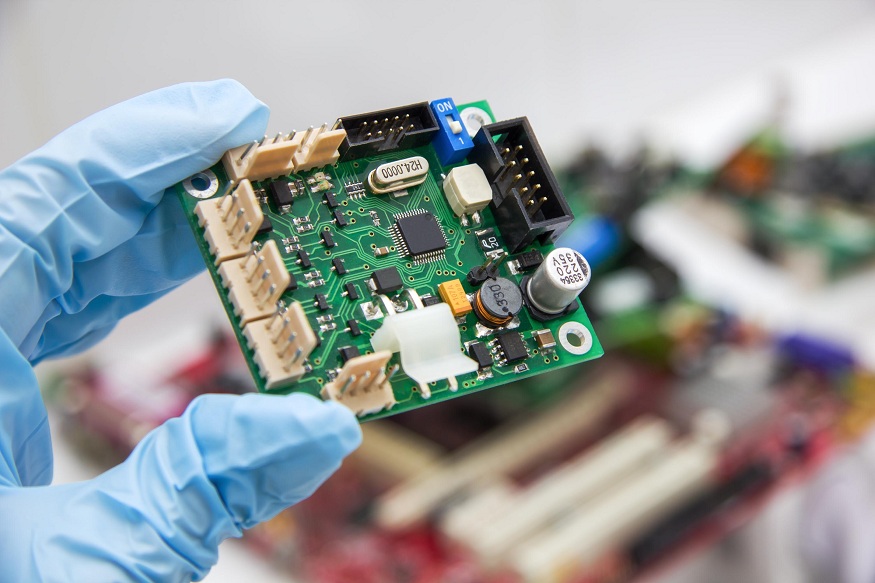
Why Complex PCB Layouts Actually Matter
Moving from a straightforward, two-layer PCB to a complicated multi-layer design changes everything. On-screen, your pcb schematic capture might look perfect. But real-world designs quickly encounter unexpected noise, grounding glitches, and heating issues.
Here’s the real deal: PCB design goes beyond electrical connections. It’s about keeping signals clean, making sure your board can actually be manufactured, and preventing overheating. In short, it’s about turning your schematic into a fully working, trouble-free product.
Managing Layers Wisely from the Start
Ever tried squeezing a dense ball-grid array onto too few layers? It’s a guaranteed headache. Smart layer management must come first—before you even draw your first trace.
Here’s what experienced engineers typically consider:
- Balancing signal, ground, and power layers carefully.
- Setting up controlled impedance for sensitive traces.
- Ensuring proper return paths for high-speed signals.
Skip these considerations, and no amount of autorouting can fix your board.
Effective Routing: More Than Just Wires and Dots
Routing brings your pcb schematic design into reality. Even the best schematics can go wrong if routing is neglected.
A few straightforward, real-world tips:
- Short, direct traces work best. Long, winding routes create interference.
- Don’t underestimate trace thickness—too thin and they’ll overheat.
- Avoid running sensitive signals across splits in ground planes.
- Keep differential pairs side by side—no exceptions.
Good routing isn’t only about placing lines. It’s about understanding signal paths and preventing unintentional interference.
Common Mistakes to Watch Out For
You’ve probably run into these before:
- Ground vias isolated without proper connectivity.
- Memory traces excessively longer than clock signals.
- Ignored design rule checks (DRCs), causing production headaches.
One frequent oversight: Not regularly checking your circuit schematic design against your PCB layout. Schematics can appear perfect, but hidden problems often surface during layout—like tight spacing or unwanted noise coupling.
Think Past the PCB Itself
Solid PCB design isn’t only about electrical performance. It’s also about aligning your electrical, mechanical, and production teams. Skipping collaboration means risking unexpected assembly or manufacturing issues.
Don’t overlook things like:
- Machine assembly constraints.
- Efficient orientation of components.
- Warping and thermal challenges during manufacturing.
Next time you’re knee-deep in multi-layer complexity, don’t just think: “Can I route this board?” Instead, ask yourself: “Will this board survive manufacturing? Will it actually work reliably? Can it scale?”
That’s how good PCB designs stand apart.